Table of Contents
- Background
- JFET
- Howland Current Source
- Design Considerations
- Summary
- Definitions
- References
- Table of Figures
- Table of Equations
Background
Current sources are a fundamental source in electronics. They are used to generate a precise current that can be applied to a system. This system is often sensors or other measurement application where the known current is used to generate a voltage which can be processed by an analog to digital converter to a digital value. This value can then be acted upon, or logged for instance. Ultimately their uses are numerous and not limited to only digital systems. They come in many forms from nano-amp current mirrors in semiconductors to kiloamps in an industrial process for plating or electrochemical cells.
An ideal current source has an infinite compliance voltage, zero output impedance and does not have dependence on the supplied voltage. In reality all of these factors limit the performance of a current source.
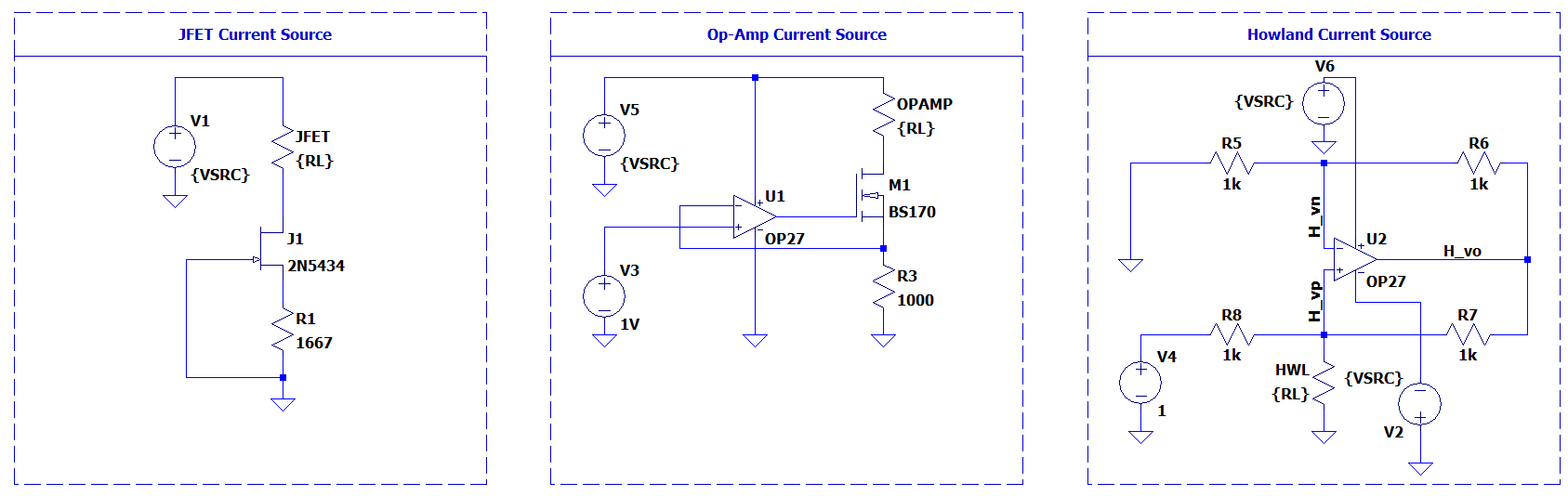
There are many different kinds of current sources. In this article the JFET and Howland architectures are discussed that have applications primarily within PCBA level designs. A simple op-amp-FET circuit is added to the simulation for comparison.
JFET

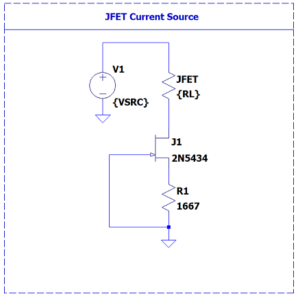
The JFET current source is one of the simplest to implement. It consists of a Junction Field Effect Transistor (JFET) and a resistor. These can also be purchased in a standalone package known as a constant current diode.
MOSFET Equivalent
A similar circuit can be implemented using a depletion mode MOSFET.
Circuit Overview
Design
The design of a JFET constant current source primarily depends on two datasheet parameters: $V_{GS(off)}$ and $I_{DSS}$. The resistor value is chosen to create the proper voltage drop, causing the JFET to conduct only the specified current.
\[\Large V_{GS} = -V_{GS(off)} \cdot \left( 1-\sqrt{\frac{I_D}{I_{DSS}}} \right)\]The required resistance can then be calculated using Ohm’s law.
\[\Large R_{DS} = \frac{V_{GS}}{I_D}\]Example Calculation
| Parameter | Value | Units |
|---|---|---|
| $V_{GS(off)}$ | -1.90 | V |
| $I_D$ | 1.0e-3 | A |
| $I_{DSS}$ | 64.90e-3 | A |
SPICE Model Usage
Component parameters can also be determined using SPICE models when datasheet values are unavailable or inconsistent. For instance the following is a model of the 2N5434 JFET. The resistor can be determined using these model parameters to match the desired current.
Note that the SPICE model parameters are typically nominal values and may not be representative of the extremes.
.model 2N5434 NJF(Beta=18m Betatce=-.5 Rd=1 Rs=1 Lambda=25m Vto=-1.9 Vtotc=-2.5m Is=.5p Isr=5p Alpha=150u Vk=110 Cgd=35p M=.4283 Cgs=35p mfg=Vishay)
where:
- $\beta$ is the transconductance parameter ($A/V^2$).
- $V_{GS}$ is the gate-source voltage.
- $V_{TO}$ is the pinch-off voltage.
- $I_D$ is the drain current.
- $I_{DSS}$ is the drain saturation current (The value of $I_D$ with $V_{GS}=0$).
Example Calculation
Using the SPICE model, the resistor can be determined as follows for a $1mA$ constant current source:
\[\Large \textcolor{WildStrawberry}{I_{DSS}} = \textcolor{Cerulean}{(0.018A/V^2)} \cdot \textcolor{BurntOrange}{(-1.9)}^2 = \textcolor{WildStrawberry}{0.06498 A}\] \[\Large V_{GS} = -(-1.90V) \cdot \left( 1-\sqrt{\frac{1\mathrm{e}{-3} A}{64.98\mathrm{e}{-3} A}} \right) =1.664V\] \[\Large R = \frac{V}{I} = \frac{1.664V}{0.001A} = 1664 \Omega\]Sensitivity
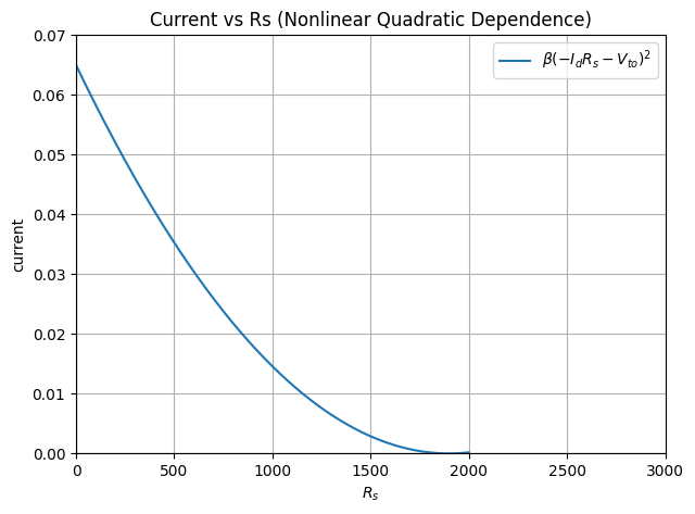
The variance due to the resistance tolerance can be calculated by rearranging the drain current equation by substituting voltage for the resistance and current. The effects of resistance change are nonlinear in nature as can be visualized on the chart.
\[\Large I_D = \beta (V_{GS} - V_{TO})^2 = \beta (-I_D \cdot R_s-V_{TO})^2\]Derivative Sign
Recall that $V_{TO}$ is negative which results in a negative value. This translates to a decreasing current with increasing resistance. Additionally, note that this equation is nonlinear.
Simulation
The JFET circuit was simulated in LTspice. It is relatively stable with changes in supply voltage but varies slightly due to channel-length modulation. 1 This channel length modulation effect is shown as an increasing curve with applied voltage.
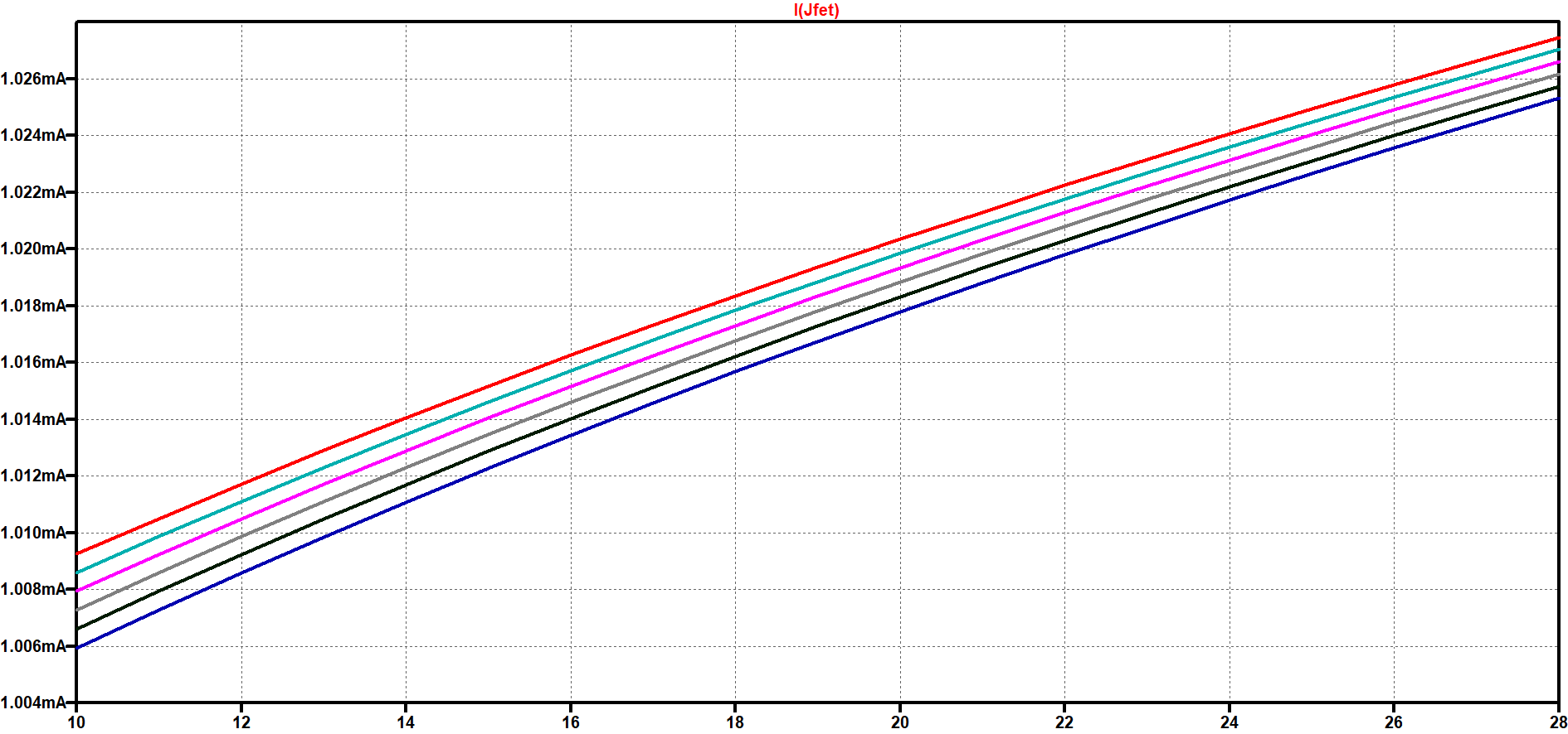
The X-axis of this plot represents the supply voltage swept from 10 V to 28 V. The Y-axis shows the current. Each color line represents a different load resistance.
Howland Current Source
The Howland current source is a voltage controlled current source using a differential feedback architecture. This architecture reduces variation from changes to power supply voltage as well as load resistance.
This implementation requires careful control over the balance of the resistors as any mismatch will result in significant deviations in output current.
Circuit Overview

Analysis
To analyze this circuit we use Kirchoff’s current rules to perform nodal analysis. Recall that Kirchhoff current law states that the sum of all currents going in and out of a circuit equal zero.
\[\Large \sum I = 0\]Additionally, the output of an amplifier is the gain of the amplifier, multiplied by the difference between the two terminals.
\[\Large V_o = A \cdot (V_p - V_n)\]Note
Ideal operational amplifiers have infinite gain. In reality this number is high, on the order of $10^6$.
The inverting input of the op-amp can be modelled as a voltage divider from the output of the op-amp.
\[\Large V_n = V_o \cdot \left( \frac{R_1}{R_1 + R_2} \right)\]Moving now to using current analysis - The non-inverting input requires summation of multiple currents.
\[\Large \frac{V_o - V_p}{R_3} + \frac{V_{in}-V_p}{R_4} - \frac{V_p}{R_L} = 0\]That is, the sum of currents through $R_3$, $R_4$, and $R_L$ equal zero. To find the current only through $R_L$ this term can be moved right hand side using algebraic manipulation.
\[\Large \frac{V_o - V_p}{R_3} + \frac{V_{in}-V_p}{R_4} = \frac{V_p}{R_L} = I_o\]Expand and factor out $V_p$
\[\Large \frac{V_o}{R_3} + \frac{V_{in}}{R_4} = V_p \left( \frac{1}{R_3} + \frac{1}{R_4} + \frac{1}{R_L} \right)\]Using op-amp properties that $V_p = V_n$ then substitute $V_o$ for the resistance equivalent.
\[\Large V_p = V_n = V_o \cdot \frac{R_1}{R_1 + R_2}\]Rearrange for $V_p$.
\[\Large V_o = \frac{R_1+R_2}{R_1}\cdot V_p\]Substitute $V_o$ for this value.
\[\Large \frac{\frac{R_1+R_2}{R_1}\cdot V_p}{R_3} + \frac{V_{in}}{R_4} = V_p \left( \frac{1}{R_3} + \frac{1}{R_4} + \frac{1}{R_L} \right)\]This equation can then be algebraically manipulated, substituting $V_p$ and $V_o$ using the prior equations.
Next, Recall that at balance the resistors are equal.
\[\Large R_1R_3 = R_2 R_4\]Simplification of the prior substituted equation results in the following equation.
\[\Large I_o = V_{in} \cdot \frac{R_1 R_3}{R_1 R_3 R_4 + R_L (R_1 R_3 - R_2 R_4)}\]Knowing that $R_1R_3$ is equivalent to $R_2 R_4$ it can be cancelled from the denominator yielding a simplified equation.
\[\Large I_o = V_{in} \cdot \frac{R_1 R_3}{R_1 R_3 R_4 + R_L \cdot 0} = V_{in} \frac{R_1 R_3}{R_1 R_3 R_4}\]It can again be simplified one step further by cancelling terms in the numerator and denominator yielding a compact equivalent.
\[\Large I_o = V_{in} \cdot \frac{1}{R_4} = \frac{V_{in}}{R_4}\]In summary at balance the relationship is as follows:
\[\Large I_o = \frac{V_{in}}{R_4}\]Sensitivity Analysis
Performing partial differentiation of the base equation results in the following equations. Note that the sign provides an intuition as to the behavior. Specifically, Increasing $R_2$ and $V_{in}$ will increase the current, whereas changing all the other inputs will decrease the output current $I_o$.
\[\Large \frac{\partial I_{O}}{\partial R_{1}} = - \frac{R_{2} R_{3} R_{4} R_{L} V_{i}}{\left(R_{1} R_{3} R_{4} + R_{1} R_{3} R_{L} - R_{2} R_{4} R_{L}\right)^{2}}\]Design Considerations
Limitations
First, a note on the design limitations. As with a typical operational amplifier there are limits to the compliance voltage as well as the power supply voltage rail margin. The current limit of the device, as well thermal management considerations.
The values must be chosen such that the resistors are not too high such that they impact the biasing condition of the op-amp.
Supply Limits
Operational amplifiers, even rail to rail devices are unable to output exactly the input supply rail. They need some margin to operate. This condition becomes the compliance limit threshold and is a limiting factor in operation.
\[\Large V_{supply} \geq V_o + V_{margin}\]Current Limit
The operational amplifier cannot output infinite current. Each device has limitations in how much current it can source or sink. For additional current a discrete output stage could be used.
Resistor Trimming
The resistors should be precision. Even 1% mismatch can cause considerable deviation. In this configuration it would be ideal to utilize a mechanism to trim the resistors for optimal matching. Temperature coefficient mismatches can also affect the output current and should be considered for best long term stability.
Thermal Management and Quiescent Power Usage
For low current applications thermal management may not be a concern, but for high current applications thermal management could become a necessity. Recall that power dissipated as heat is proportional to the square of the current and the resistance. The resistors chosen therefore impact both the system thermal performance as well as the quiescent power usage.
\[\Large P_{diss} = I^2 R\]Compliance Limit
Note that in this particular Howland configuration there is a voltage divider effect with equal resistors. This means that the output to the load will be half the output from $V_o$. This significantly reduces the maximum available compliance voltage from the op-amp.
\[\Large I_o \leq \frac{0.5\cdot V_{o(max)}}{R_L}\]where $V_{o(max)}$ would be something on the order of $(V_s - V_{margin}) / 2$. Where the margin would be the maximum rail-rail operational headroom required from the op-amp. The factor of 2 accounts for the voltage divider. This factor would change if the resistors were no longer equal.
Improved Howland
Note that in the improved Howland configuration these effects are mitigated.
Additional Considerations
The Howland design needs an operational amplifier with a high common mode rejection ratio, low bias current, and low offset voltages. These will directly impact the system mismatch and should also be considered for critical designs.
Component Value Calculation
| Requirement | Symbol | Description |
|---|---|---|
| Output Current | $I_o$ | Desired maximum output current. |
| Control Voltage | $V_{in}$ | Maximum control voltage to calculate current output. |
| Allowable Error | $\epsilon_I$ | Allowable current error, used to determine required tolerance. |
| Load Resistance | $R_L$ | Maximum load resistance, to determine compliance voltage. |
Summary
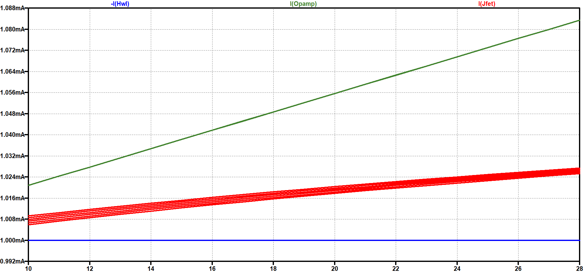
Three current source architectures were simulated with a $1mA$ current target. The JFET was the simplest to implement utilizing only two components. The JFET suffers from variation due to the intrinsic channel length modulation characteristics of the device as well as slightly due to the load resistance. The Op-Amp produces nearly no variation due to change in load, however suffers the most from change in supplied voltage. Ultimately the Howland under ideal conditions performs the best with near zero change in output current with a change in applied voltage or variation in load resistors over the chosen range.
Definitions
| Term | Description |
|---|---|
| CMRR | Common Mode Rejection Ratio |
| JFET | Junction Field Effect Transistor |
| Op-Amp | Operation Amplifier |
| MOSFET | Metal Oxide Semiconductor Field Effect Transistor |
References
| Reference | Description |
|---|---|
| AN-1515 A Comprehensive Study of the Howland Current Pump | Technical whitepaper detailing the operational details of the Howland current pump. |
| Wikipedia - Constant Current Diode | Additional details of the constant current diode. |
| Georgia Tech - The JFET | Explanation of JFET with formulas. |
| LTspice | SPICE Circuit Simulator |
Table of Figures
- LTSpice Simulation Schematic
- JFET Semiconductor Structure
- JFET Load Resistance Sensitivity Plot
- JFET Simulation Circuit
- JFET Simulation Results, Current vs Applied Voltage
- Howland Current Source Circuit
- SPICE Simulation Schematic
- SPICE Simulation Summary, Output vs Input Voltage
Table of Equations
- JFET Gate Source Voltage
- JFET Drain Resistance
- Drain Current
- Drain Saturation
- JFET Drain Current
- JFET Drain Current vs Load Resistance Derivative
- Kirchoff’s Current Law
- Differential Amplifier Equation
- Op-Amp Inverting Node Voltage
- Circuit Current Summation, Non-Inverting Node
- Output Current Derivation
- Output Current Derivation, Expanded and Factored
- Positive Node Equivalence Derivation
- Output Voltage Derivation
- Substituted Intermediate Step
- Resistance Equivalence at Balance
- Howland Output Current Equation
- Simplifying Steps for Output Current Equation at Balance
- Simplified Output Current Equation at Balance
- Company Simplified Current Equation at Balance
- Howland Partial Derivative, Output vs R1
- Howland Partial Derivative, Output vs R2
- Howland Partial Derivative, Output vs R3
- Howland Partial Derivative, Output vs R4
- Howland Partial Derivative, Output vs Load Resistance
- Howland Partial Derivative, Output vs Input Voltage
-
https://en.wikipedia.org/wiki/Channel_length_modulation ↩