Table of Contents
Introduction
A linear voltage regulator is a device which reduces and regulates an output voltage by creating a voltage differential. There are several architectures of linear regulators such as series and shunt. This article will focus on the most common topology, the series topology.
The series topology uses a series pass transistor to regulate the voltage. This circuit operates similarly to a voltage divider but will actively control the resistance to keep the output voltage at a desired setpoint. This circuit does this by controlling the gate voltage of a P-channel MOSFET.
In this article both static and active regulation models are discussed and some key detailed analysis are included to provide a high level understanding of the operational principles of the linear voltage regulator.
Simulation files are provided for those who wish to replicate the calculations and tweak parameters for a better understanding. Topics such as PSRR, stability analysis, and compensation network calculations have been omitted for this introduction.
Static Ideal Model
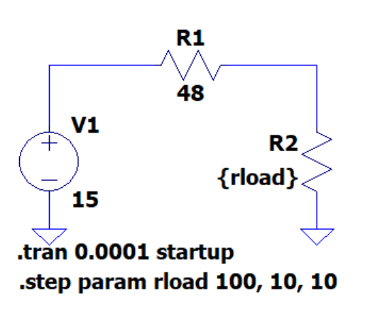
Consider a circuit in which all parameters are fixed, purely resistive, using ideal components. That is, there is no consideration given to self-heating, manufacturing tolerance, and so on. Provided this, a linear regulator at a single point can be modelled as a voltage divider.
Parameters
- Input voltage: 15V
- Output voltage: 3V
- Load resistance: 12\(\Omega\)
Model Synthesis
To synthesize a mathematical model of a voltage divider the parameters are used. The load resistance forms \(\textcolor{WildStrawberry}{R_2}\). Since the input voltage and output voltage are known these parameters can be inserted into the voltage divider formula which is then rearranged to obtain a formula solving for \(\textcolor{Cerulean}{R_1}\).
\[\Large V_{out} = V_{in} \cdot \frac{\textcolor{WildStrawberry}{R_2}}{\textcolor{Cerulean}{R_1} + \textcolor{WildStrawberry}{R_2}}\]Algebraic Steps
The following is a step-by-step method to rearrange the terms to solve for \(\textcolor{Cerulean}{R_1}\).
Step 1: Divide both sides by \(V_{in}\)
\[\Large V_{out} = V_{in} \cdot \frac{\textcolor{WildStrawberry}{R_2}}{\textcolor{Cerulean}{R_1} + \textcolor{WildStrawberry}{R_2}} \rightarrow \frac{V_{out}}{V_{in}} = \frac{\textcolor{WildStrawberry}{R_2}}{\textcolor{Cerulean}{R_1} + \textcolor{WildStrawberry}{R_2}}\]Step 2: Invert both sides so that the \(\textcolor{WildStrawberry}{R_2}\) term is in the denominator.
\[\Large \left( \frac{V_{out}}{V_{in}} \right)^{-1} = \left(\frac{\textcolor{WildStrawberry}{R_2}}{\textcolor{Cerulean}{R_1} + \textcolor{WildStrawberry}{R_2}} \right)^{-1} \rightarrow \frac{V_{in}}{V_{out}} = \frac{\textcolor{Cerulean}{R_1} + \textcolor{WildStrawberry}{R_2}}{\textcolor{WildStrawberry}{R_2}}\]Step 3: Multiply both sides by \(\textcolor{WildStrawberry}{R_2}\)
\[\Large \frac{V_{in}}{V_{out}} \cdot \textcolor{WildStrawberry}{R_2} = \frac{\textcolor{Cerulean}{R_1} + \textcolor{WildStrawberry}{R_2}}{\textcolor{WildStrawberry}{R_2}} \cdot \textcolor{WildStrawberry}{R_2} \rightarrow \frac{V_{in}}{V_{out}} \cdot \textcolor{WildStrawberry}{R_2} = \textcolor{Cerulean}{R_1} + \textcolor{WildStrawberry}{R_2}\]Step 4: Subtract \(\textcolor{WildStrawberry}{R_2}\) from both sides
\[\Large \frac{V_{in}}{V_{out}} \cdot \textcolor{WildStrawberry}{R_2} - \textcolor{WildStrawberry}{R_2} = \textcolor{Cerulean}{R_1} + \textcolor{WildStrawberry}{R_2} - \textcolor{WildStrawberry}{R_2} \rightarrow \frac{V_{in}}{V_{out}} \cdot \textcolor{WildStrawberry}{R_2} - \textcolor{WildStrawberry}{R_2} = \textcolor{Cerulean}{R_1}\]Result:
\[\Large \textcolor{Cerulean}{R_1} = \frac{V_{in}}{V_{out}} \cdot \textcolor{WildStrawberry}{R_2} - \textcolor{WildStrawberry}{R_2}\]This equation can now be used to solve for the \(\textcolor{Cerulean}{R_1}\) resistor needed to achieve the desired output voltage.
Example Calculation
Given that the supply voltage is 15V, the desired output voltage is 3V, and the purely resistive ideal load is \(12 \Omega\) the calculated value for \(R_1\) can be found as follows:
\[\Large \textcolor{Cerulean}{R_1} = \frac{15V}{3V} \cdot 12 \Omega - 12 \Omega = \textcolor{Cerulean}{48 \Omega}\]Static Model Challenges
The static model works for a single load resistance with a single input voltage. When either of these parameters change so does the output voltage. The solution to this is to add active control to regulate the output. This can be done with a transistor and an operational amplifier but first to illustrate how a shift in supply voltage changes the output, the calculation can be performed again with the shift.
Assume the supply decreases by \(1.0V\). The output will also decrease linearly proportional to the voltage change:
\[\Large V_{out} = (15V - 1.0V) \cdot \frac{\textcolor{WildStrawberry}{12\Omega}}{\textcolor{Cerulean}{48\Omega} + \textcolor{WildStrawberry}{12\Omega}} = 2.8V\]Since the system is linear in nature, the shift can also be calculated using the partial derivative of the output voltage with respect to the input voltage. That is, for each volt of input voltage change the output will shift according to the ratio of the voltage divider. In this case, \(200mV\) shift for each volt change.
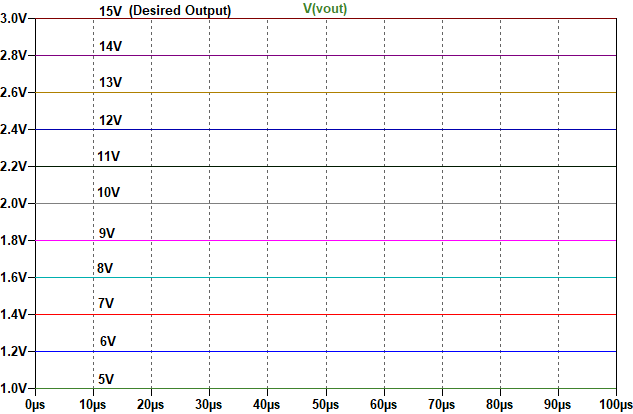
\[\Large \frac{\partial V_{in} \cdot \frac{\textcolor{WildStrawberry}{R_2}}{\textcolor{Cerulean}{R_1} + \textcolor{WildStrawberry}{R_2}}}{\partial V_{in}} = \frac{\textcolor{WildStrawberry}{R_2}}{\textcolor{Cerulean}{R_1} + \textcolor{WildStrawberry}{R_2}} = \frac{\textcolor{WildStrawberry}{12}}{\textcolor{Cerulean}{48}+\textcolor{WildStrawberry}{12}} = 0.2 V/V\]A simulation of this result is shown below where each subsequent trace represents a 1V shift in the input voltage starting from 15V. The Y axis represents the output of the power supply. The X-axis represents time however can be ignored since this is a DC steady-state simulation using ideal components.
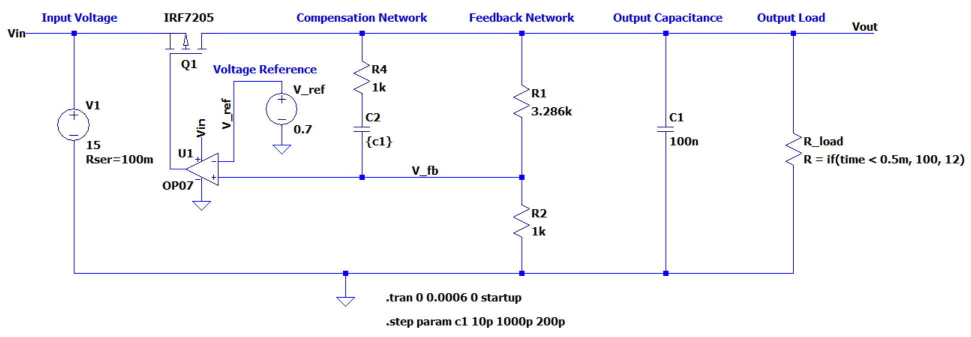
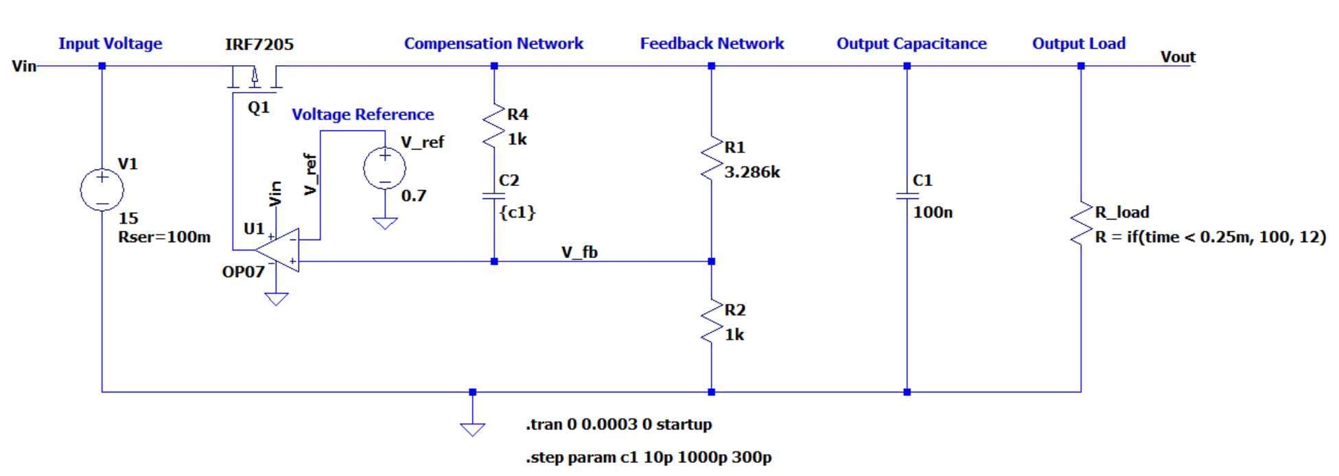
Active Regulation Model

Instead of a single resistor for \(\textcolor{Cerulean}{R_1}\), an active element (transistor) allows changing of the resistance to achieve the desired output voltage. This example focuses on the use of an enhancement type P-channel MOSFET. A linear regulator can be constructed with both N and P type MOSFETS as well as bipolar junction transistors (BJT) however the implementation will differ slightly for each. For instance an N-channel topology may have lower \(R_{DS_{ON}}\) however, the gate voltage must be \(V_{th}\) above the source terminal to turn on. A bootstrap circuit such as a charge pump would allow greater operating ranges.
The minimum required elements to construct a linear series regulator are:
- Transistor - responsible for controlling resistance to regulate the output voltage.
- Operational amplifier (“Op-Amp”) - responsible for controlling the transistor.
- Voltage reference - sets a known point for comparison.
- Feedback network - shifts the output voltage down to the voltage reference level.
In the real world it may be helpful to consider some elements such as:
- Decoupling capacitors - stabilizes operation of the op-amp.
- Compensation network - enhances operation and prevents oscillations.
- Output capacitance - stabilizes the output and reduces ripple.
- Series gate resistor - dampens oscillations.
- Gate pull-up resistor - expands operational range for low output voltages.
Intuitive Operational Principles
Before diving into the technical operational details of the active linear regulator it is helpful to gain an intuitive understanding of each of the blocks involved.
A P-channel MOSFET is active, or conducting, when the voltage at the gate exceeds the threshold voltage, typically specified in datasheets as \(V_{GS_{(th)}}\). This is specified as a negative voltage for P-Channel MOSFETs. What this means is the gate must be at a lower voltage potential than the source of the FET to begin conducting. This communicates how to setup the operational amplifier to control the transistor.
Next, an operational amplifier is used in conjunction with a feedback network and a voltage reference. The voltage reference is a known voltage to compare the measured output voltage against. It could be any point within input range of the op-amp, but is usually a relatively small voltage and will impact the minimum output voltage possible for the regulator.
Since the P-FET is not conducting (“high resistance”) when the gate is at its maximum voltage the feedback network is connected to the non-inverting input since when the threshold voltage exceeds the reference the output of the op-amp will increase. This translates to increasing the resistance of the FET until it it back in regulation. In contrast, the voltage reference is connected to the inverting input. This means that the op-amp’s output will decrease in voltage until the feedback network is equal to the inverting input voltage. This translates to the P-FET decreasing in resistance.
For clarity, it may be helpful to remember the open loop operation of an op-amp which functions as a comparator. In this case an op-amp will output the voltage from the pin that has the highest voltage. That is to say if the non-inverting input (“+”) is higher than the inverting input (“-“) the output will be positive. However, if the output at the inverting pin (“-“) is higher with respect to the other input then the output it will be negative. A helpful mnemonic since an op-amp looks like a triangle (“open alligators mouth”) is “the alligator eats the larger number” just like in basic math.
In summary for a P-FET architecture:
- Increasing \(V_{GS}\) increases resistance, which translates to lower output voltage.
- Decreasing \(V_{GS}\) decreases resistance, which translates to higher output voltage.
Detailed Analysis
Efficiency
The efficiency of a linear regulator is typically denoted as \(\eta\), the Greek letter “eta”. Linear regulators are never 100% efficient because they create a voltage differential which causes the system to dissipate excess power.
The efficiency is simply expressed as a ratio of output power to input power.
\[\Large \eta = \frac{P_{out}}{P_{in}}\]Neglecting power consumed by the Op-amp, and secondary circuits within the voltage regulator we can calculate the efficiency of our circuit:
\[\Large \frac{3V \cdot 0.25A}{15V \cdot 0.25A} = \frac{0.75W}{3.75W} = 20\%\]Notice how current input is equal to current output. While in reality the efficiency will be slightly less due to power consumed by the op-amp, voltage reference, and other devices it serves an as approximation.
Since most of this power will be dissipated in the MOSFET the approximate thermal rise can be calculated for the specific transistor:
\[\Large T_{amb} +3W \cdot 50 ° C / W = 25 ° C + 3 \cdot 50 =175 ° C\]Note that the parameter \(50 ° C / W\) is the junction-ambient specification on the datasheet for the MOSFET used. The \(25 ° C\) is approximate ambient temperature.
This exceeds both the maximum power dissipation (2.5W) of the transistor as well as the maximum junction temperature. This means that a different device is needed, and often a heatsink in the case of linear regulators. The input voltage can also be decreased. If for instance the same device was operated from a 5V rail instead the power dissipation would be substantially different:
\[\Large \eta = \frac{3V \cdot 0.25A}{5V \cdot 0.25A} = \frac{0.75W}{1.25W} = 60\%\] \[\Large 25 ° C + 0.5W \cdot 50 ° C/W = 50 ° C\]Notice also how the simulation does not inform one that the power dissipation has been exceeded. This is why boundary conditions are needed to ensure a system works as expected.
Op-Amp Output Limits (“Saturation”)
In the real world components are not ideal. Even “rail to rail” op-amps have some deviation between them and the voltage rail. If the op-amp cannot output sufficient voltage to drive the P-FET into a high resistance state then there may be issues with regulating to lower voltages. To mitigate this placing a resistor between \(V_{in}\) and the MOSFET gate will allow the gate capacitance to charge to a higher voltage ensuring it is off when needed. This could alternatively be another transistor to minimize quiescent operational current.
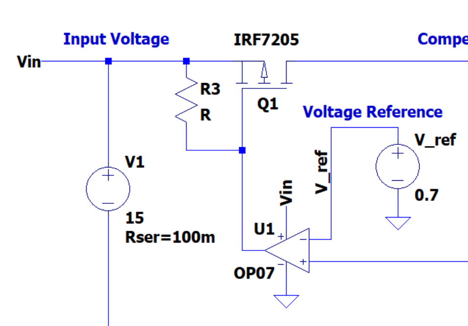
Note the location of R3 where the resistance would be chosen such that it keeps the MOSFET gate charged when the op-amp is near it’s high saturation limits.
Gate Charge
The MOSFET will have a gate charge associated with it that can lead to oscillations as well as a phase shift due to the time it takes to charge the MOSFET gate. Adding a gate resistor can dampen oscillations caused by ringing in high speed applications (as well as slow the response time). Additionally, adding a compensation network (resistor and capacitor in series) will help minimize oscillations due to a step response.
Recall that the charge on a MOSFET is specified in terms of coulombs, typically nanocoulombs (\(nC\)). This is a voltage dependent quantity.
\[\Large C = \frac{q}{V}\]where:
- \(C\) is capacitance in Farads.
- q is charge in Coulombs.
- V is applied voltage, in Volts.
For example, if the gate of the IRF7205 with a 40nC maximum charge is charged to a voltage of 15V then the capacitance would be:
\[\Large \frac{40e-9 C}{15V} = 2.667e-9F = 2.667nF\]Then, applying the RC time constant:
\[\Large V_{cap} = V_{s} \cdot \left( 1 - e^{(-t/R\cdot C)} \right )\]Where the resistance of the OP07 is approximated as 750\(\Omega\) from \(20mA\) output current and drive voltage of \(15V\). The time constant for this circuit is then \(2.667nF \cdot 750 \Omega = 2\mu s\). To charge to 95% it will require \(3 \tau\) (time constants) or in other words \(6\mu s\). To decrease this an op-amp with higher output current or a FET with a lower gate charge can be used. In reality the transition time will be faster for the FET since it is less likely to have step from no charge to full charge.
Dropout Voltage
The dropout voltage is a parameter of a linear regulator which describes the minimum voltage across the regulator in order to maintain output regulation. This can be a critical parameter when the margins are small such as converting between from a 3.7V nominal battery to 3.3V or similar small voltage differentials.
While each topology is unique in its dropout characteristics, this simplified model consisting of a series P-channel FET has a dropout voltage minimum as a function proportional to the MOSFET on resistance.
With a maximum current of \(250mA\) the voltage across the FET will then be:
\[\Large V = 0.25A \cdot 130\text{e}\!-\!3 \Omega = 32.5mV\]The dropout voltage will then be a function of the voltage across the FET as well as the margin necessary to maintain a regulated output within a specified tolerance. The \(32.5mV\) becomes a boundary condition in which the device output will always be that much lower than the input for the specified current.
Op-Amp Slew Rate
The slew rate of the operational amplifier is a measure of how fast the output can change “slew” for a given commanded voltage. If commanded an ideal step (square wave) the slew rate will make the output appear as a slope instead of a sharp rising edge. This is also referred to as “slew rate limited”.
\[\Large t_{slew} = \frac{\Delta V}{\text{SR} \frac{V}{\mu s}}\]where:
- \(\Delta V\) is the step magnitude, in volts.
- \(SR\) is the slew rate in units of \(\frac{V}{\mu s}\).
The OP07 has a minimum slew rate specification of \(0.1 \frac{V}{\mu s}\) with \(0.3 \frac{V}{\mu s}\) being typical. Assuming a step from 0V to 15V the time it will take to change will be on the order of \(50\mu s\). Given that the FET gate time constant is substantially smaller than this, the circuit response time will be limited by the Op-Amp slew rate.
\[\Large t_{slew}=\frac{15-0}{0.3 \frac{V}{\mu s}} = 50\mu s\]Note that the slew rate for this Op-Amp is specified under different conditions, and the values used were typical, not minimums. This means that the guaranteed or worst case conditions of this Op-Amp could be much slower.
Output Capacitance
The addition of an output capacitance will help reduce ripple voltages and aid in ensuring the circuit stays regulated as the load changes.
Op-Amp Offset Voltage
Operational amplifiers will have some offset voltage specifications that will introduce a DC offset (“error”) in the output voltage. This offset can be modelled as a voltage source in series with the input terminals. The offset could be positive or negative and depends on the device used. Offset can be compensated by trimming the feedback network for each device. If the offset voltage is a critical parameter then selecting an op-amp with a low offset voltage would be ideal.
The offset voltage will shift the DC output by the inverse of the feedback network. For example using the simulation example and the voltage divider equation:
\[\Large V_{error} = V_{offset} \cdot \left( \frac{3.286k \Omega}{3.286k \Omega + 1k \Omega} \right ) ^{-1}\] \[\Large = V_{offset} \cdot \left( \frac{3.286k \Omega + 1k \Omega}{3.286k \Omega} \right ) = V_{offset} \cdot 1.304\]Since the voltage divider divides down the output voltage it essentially adds a gain factor at the output voltage node. For this circuit, it means that every 1mV offset will correspond to a 1.304mV shift at the output.
Part Tolerances and Environmental Effects
In additional to the outlined non-idealities part tolerance need to be considered. Components have specified tolerances, such as resistors 1-5% are typical. Additionally, there are thermal effects that will induce parameter shifts in both passive and active components. Devices also dissipate heat causing additional \(\Delta T\) to occur.
Simulation
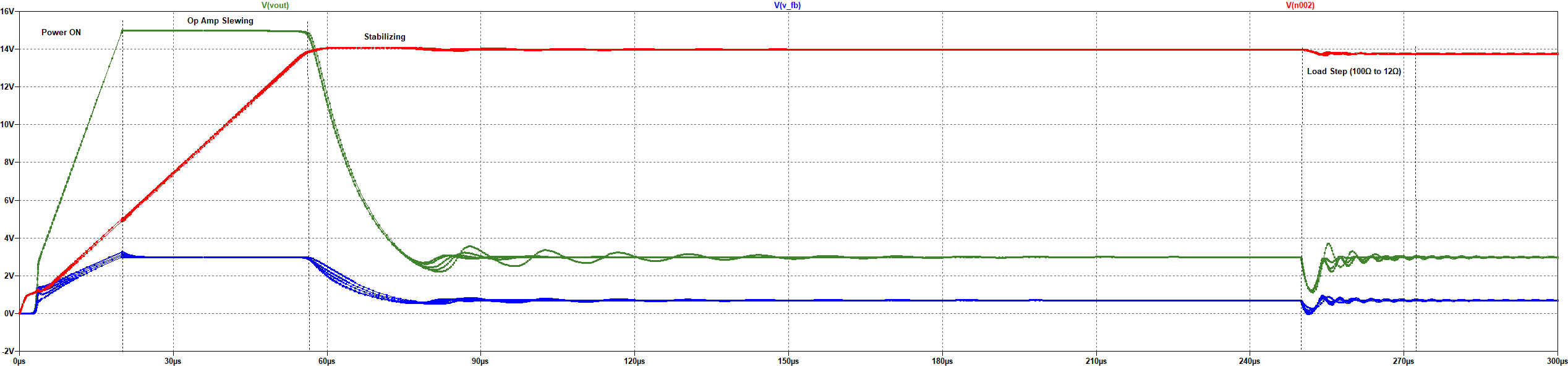
To illustrate how the circuit performs a transient simulation has been done. This simulation steps through values of compensation capacitance with a load step from \(100 \Omega\) to 12 \(\Omega\). The approximate time intervals have been labelled.
The red trace is the gate voltage. Notice how the op-amp cannot output the positive rail voltage and is instead reduced slightly. This can be compensated for by adding a resistor from the input rail to the FET gate.
The green trace is the output voltage. The target is 3.0V. There are some oscillations due to the phase delay primarily due to the circuit capacitance. In this trace is several stacked simulations which represent increasing the compensation capacitance. As the compensation capacitance reaches maximum note how the oscillations are significantly dampened.
The blue trace is the feedback voltage measured at the noninverting input of the op-amp.
Finally, note the load step that has been generated at \(25\mu s\). This shows the step response behavior of the circuit in the time domain.
Summary
In Summary, The response time of this type of linear regulator is governed primarily by the op-amp. Contributions to response time also include the compensation network, as well as the gate charge of the P-channel MOSFET. Linear regulators are a good solution when voltage differential is minimal due to the efficiency loss and power dissipation required at higher power differentials.
Simulation Files
The following are LTSpice simulation files. They were created with LTSpice 17.1.11.