Overview
In this article we discuss the design of a Form-A reed relay based multiplexer for test and measurement applications.
Table of Contents
Background
Multiplexers are a highly useful device to expand the capability of existing equipment by allowing a single instrument to programmatically connect (or disconnect) upon command. Typically a multiplexer requires a mainframe and are sold individually as cards in the case of PXIe systems. They tend to be relatively expensive for what they are and often times you want to use a significant number of channels which add up quickly. Given that I have a frequent need for multiplexers I have taken the opportunity to design my own standalone compact unit.
For this application I needed to be able to interface my Keithley DMM6500 and function generator to multiple signals for an automated test to use in qualification of some electronics designs. Most of the outputs are anticipated to be DC or certainly less than 1MHz so bear in mind this is not an RF multiplexer.
The general requirements chosen for this project include:
- USB-C compatible
- Platform independent interface
- LED indicators for visual confirmation
- Banana plug output to connect to existing test leads
- Quick connect method for reconfigurability
- Long lifetime
- Compact size and low power usage (“USB Powered”)
Component Choices
Controller
The controller chosen for this project was an ARM microcontroller. Specifically the Microchip SAMD51G19A. This is a 48QFN packages IC that has built in USB support and a maximum clock frequency of 120MHz. These are around $5 each in small quantities and I keep stock of them for projects such as this. Other microcontrollers, especially lower cost could be used, but most don’t have USB which means adding an FTDI chip which gets you to essentially the same price point.
Alternatively, you could potentially use one of the FTDI chips with an I2C or SPI port expander, or even bit bang the data lines. That however would require host software to control the device which is something I wanted to avoid for this project so that it can be used on any platform as a standard serial port device.
Relays
Relays come in many different types, however, since we want to have our relays last as long as possible reed relays are typically the go-to for small signal applications (low current). This is because reed relays have actuations rated in the millions (or billions) of cycles. If you carefully observe datasheets like those from Coto you will find that the configuration of the relay also greatly impacts the cycle count. Form A (SPST) relays often times have a significantly higher cycle rating than a form C (SPDT).
Reed relays usually use a sealed glass ampoule with a coil wound around it to actuate the relay. There are different winding schemes (and material options) depending on thermal EMF, contact form, and so on. One of the most prominent manufacturers of reed relays it Coto Technology. They are well known in the industry for having an excellent product but are no means the only one. I have used products from Pickering, Coto, and Littelfuse with good results to name a few. Coto tends to be my favorite because they make their documentation and 3D models so easy to access.
Connectors
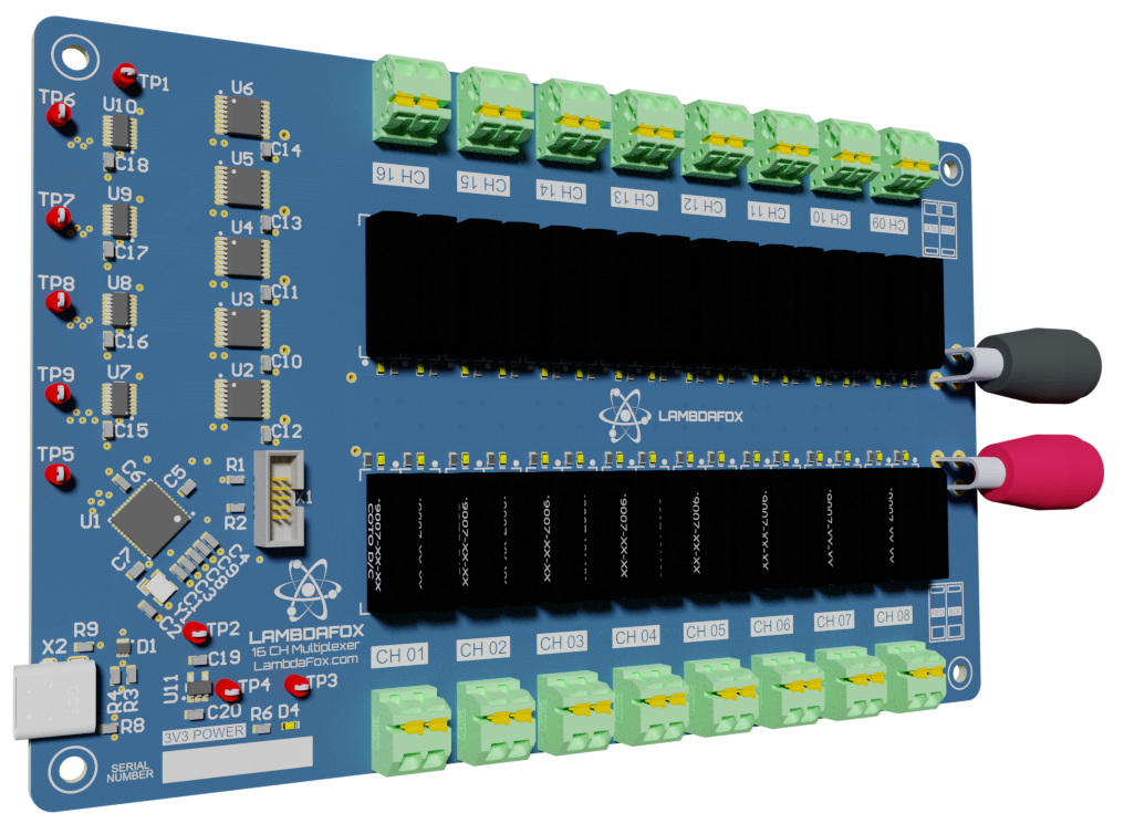
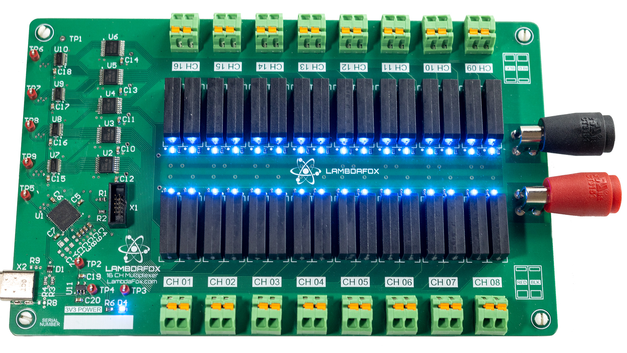
When it comes to connectors I wanted some form of quick connection. I’m a huge fan of ferrules on all my cable harnesses for loose ends because they stand up longer over time so naturally I went with push in spring loaded terminals. This makes the connections very easy to install by just pressing in the ferrule, and releasing by pressing the actuator with a flat blade screwdriver. Screw in terminal block are take substantially more effort and time to install. The specific connectors I went with for this project are from Phoenix Contact. Specifically, Part number 1861933 which is rated for 160V 16A. These are my go-to for designs that require good mechanical attachment since they have 2 pins per contact and tend to be low profile and durable. While there are likely smaller available these are still easy to use with your hands and don’t take up too much board space.
Shift Register
Shift registers allow the design to use less GPIO since we are driving 32 individual relays so we don’t want to have to buy a larger MCU to control all of the signals. Shift registers allow us to expand our IO substantially with just a few pins for clock, data, and enable. For this specific design I went with the SN74HCS595DYY. This is an 8-bit shift register with schmitt-trigger input and a tristate output. An alternative solution would be to use an I2C or SPI expander IC but the 595’ is much cheaper at about a quarter each $0.25 and come in very small footprints to save on board space.
Relay Drivers
Usually you don’t want to drive an inductive load (relay coils) directly from GPIO including that of a shift register. For switching inductive loads you also want a kickback diode. These are diodes placed inverse to the flow of current to catch reverse EMF spikes when the inductor turns off. For this I used a simple darlington transistor array which happens to have diodes built in. Specifically the ULN2003APW. Another nice feature of these is that they even have a built in base resistor which saves on board space and BOM cost.
Implementation
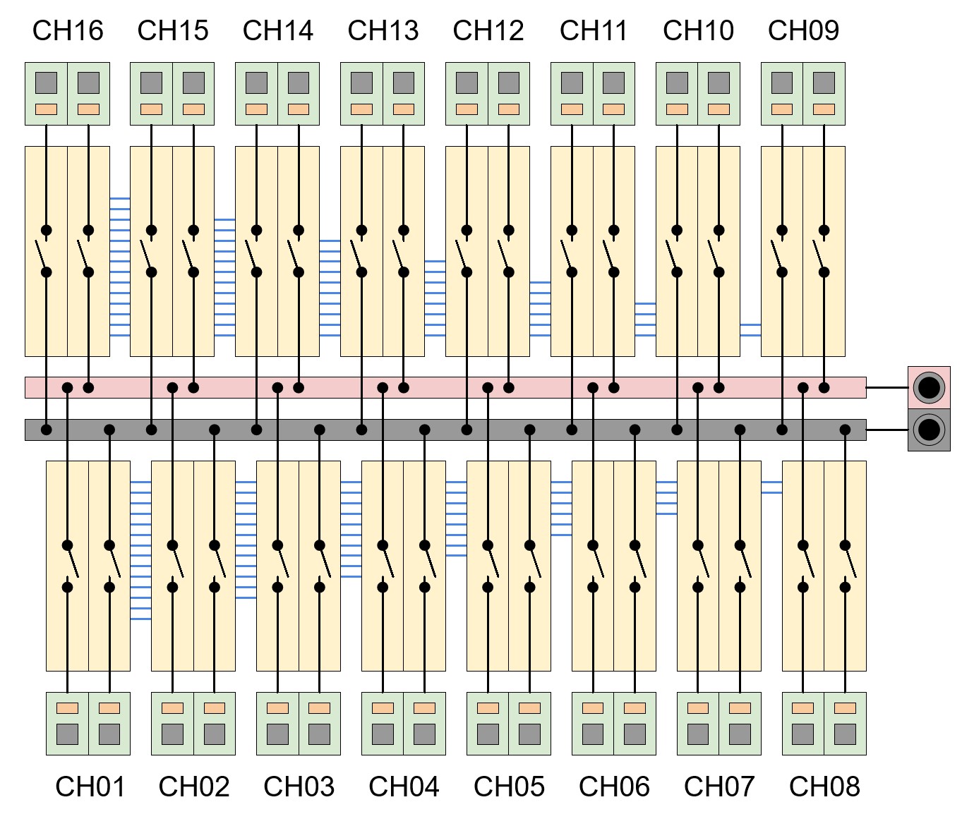
This multiplexer was implemented with a Form-A relay which means each relay is an individual switch. What that allows is fault injection for testing. Specifically, you can disconnect either the high or the low connection to test how the system performs. Additionally, there is a common bus that all the relays connect to which allows short circuit testing to occur, or simultaneous signal injection depending on the use.
For a specific example, if you take a look at my digital isolator design it has 16 channels. This was one of the motivations in designing this multiplexer is to support fully automated testing of isolator devices. So with this design I can connect all 16 channels, excite them simultaneously using a function generator and investigate phase to phase variance between the channels for instance. I can then disconnect one channel and measure crosstalk, inject a fault on one channel while observing others and so on.
Layout Elements
Channel Status Indication
I am a huge fan of indicators and like to add them everywhere. Most of the time board space as it pertains to indicators is of minimal concern. This is because they are so small but even if BOM costs are a concern they can be noted as do not populate for production. Having indicators for both power as well as each channel’s relay states allow for quick debugging and verification of events and state. They also just look cool and add a bit of flair to your device. The LEDs on this board consume less than a milliamp each when activated and are a bright blue color.
Test Points
I try to add test points to all critical connections. For this design I do think I added too few points. In retrospect I would have liked to breakout addition unused IO such as as UART connection for debugging, and some spare GPIO as well to aid in troubleshooting. I was able to finish the software without this, but it would have made things a bit easier to troubleshoot when USB wasn’t working right. Suffice to say a logic analyzer was critical for this project to confirm code was writing the expected values to the shift register chain.
Silkscreen
Silkscreen is an important design element that I frequently see other designers disregard. On many products I have seen cryptic text that requires a magnifying glass to even see. I have found that I prefer to use inverted text for important aspects. That is, items that a user will be needing to read or understand. This would be things like channel identification numbers and so on. Silkscreen can also be used to add drawings, and diagrams to a design. You can see for example both sides have a connection diagram noting which side goes to what banana jack. You should always strive to make your product as easy and as intuitive as possible to use. Silkscreen is one of the tools as our disposal to make that happen.
Firmware
The embedded firmware for this project was written in C using the ASF framework which includes an abstraction layer for configuration, GPIO, USB and so on. This has since been discontinued in favor of MPLAB Harmony but I still prefer using the original Atmel Studio IDE because I find it more intuitive and easier to use.
The firmware has three main parts to it:
- USB interface
- Command parser
- Relay logic
USB Interface
The USB interface is built into the SAMD51. From the hardware standpoint it is a through-hole USB-C connector that has ESD diodes and has series 22Ω resistors and connectors directly to the IC. Once on the device the middleware used is the CDC ACM driver. This handles serial port emulation and provides a CDC demonstration and generates a usb_start.c and usb_start.h files respectively. The example method cdcd_acm_example() echos everything you send to the device and should be enough to get you started in building your final driver.
One thing to remember is that you never know when a message will appear on the USB bus so the system must always be “available” to receive it. I found that writing back to the serial bus from the MCU side is relatively easy, but reading can be involved. I have found that callbacks are necessary and that the example leaves a lot to be desired. For example if you want to read back in a single operation more than 64 bytes you need to look into buffering multiple frames. Circular or ring buffers come up when you start looking into this. For now since the commands for this system are short extended functionality for longer messages is not needed.
The provided example code for reference is as follows:
/**
 * Example of using CDC ACM Function.
 * \note
 * In this example, we will use a PC as a USB host:
 * - Connect the DEBUG USB on XPLAINED board to PC for program download.
 * - Connect the TARGET USB on XPLAINED board to PC for running program.
 * The application will behave as a virtual COM.
 * - Open a HyperTerminal or other COM tools in PC side.
 * - Send out a character or string and it will echo the content received.
 */
void cdcd_acm_example(void)
{
	while (!cdcdf_acm_is_enabled()) {
		// wait cdc acm to be installed
	};

	cdcdf_acm_register_callback(CDCDF_ACM_CB_STATE_C, (FUNC_PTR)usb_device_cb_state_c);

	while (1) {
	}
}
Command Parser
The command parser is a simple search algorithm that is bounded by delimiters. It searches for both a command and a value. For example if sent <HELLO:123> it would extract HELLO as the command and 123 as the value. Both of these are extracted as characters so conversion such as atoi() may be needed. There are more sophisticated methods of implementing this, but this is relatively simple and can be written and validated in short time. It also works quite well for this application.
struct command{
	char command[64];
	char value	[64];
};
typedef struct command command_t;

command_t parse(char *inputString, char sDelimit, char valDelimit, char eDelimit){
	bool copyFlag 	= 0;
	int copy_ndx 	= 0;
	char buffer[64] = "";
	command_t parsed_data = {0};

	for(int i = 0; i < strnlen(inputString, 32); i++){
		if(inputString[i] == sDelimit){
			copyFlag = 1;
			i++;
		}
		else if(inputString[i] == eDelimit){
			copyFlag = 0;
		}
		if(copyFlag){
			buffer[copy_ndx] = inputString[i];
			copy_ndx ++;
		}
	}

	int ndx_sep = 0;
	for(int i = 0; i < strnlen(buffer, 50); i++){
		if(inputString[i] == valDelimit){
			ndx_sep = i;
		}
	}

	for(int i = 0; i < ndx_sep; i++){
		if(buffer[i] == valDelimit){
			break;
		}
		else{
			parsed_data.command[i] = buffer[i];
		}
	}

	int walk_ndx = ndx_sep;
	int command_ndx = 0;
	while(buffer[walk_ndx] > 0){
		parsed_data.value[command_ndx] = buffer[walk_ndx];
		walk_ndx ++;
		command_ndx++;
	}
	return(parsed_data);
}
Relay Logic
The relay logic was written as a simple bit-shifting program and the data constructed of a relay configuration struct. Each channel has it’s own status, and configuration variables. It is then extracted into a 32-bit unsigned integer. Once extracted the values are all shifted out to the serial line of the shift register. That looks something like this:
void write_relay_states(relay_ch_s *config[16]){
	uint_fast32_t relay_state = 0b0;

	for(int channel = 0; channel < 16; channel++){
		if(config[channel]->red){
		relay_state = relay_state | config[channel]->red_addr;
	}
		if(config[channel]->black){
		relay_state = relay_state | config[channel]->black_addr;
		}
	}
	for(int i = 0; i < 32; i++){
		bool bit = (relay_state >> i) & 1;
		write_serial_bool(bit);
		strobe_serial_clock();
	}
	strobe_register_clock();
}
As mentioned each relay has it’s own address because they are not necessarily sequenced in numerical order. This was done to make a cleaner and better PCB layout. Sometimes considering the software implementation and what can and cannot be worked in software can truly help a PCB layout. For instance between the 8 channel grouping the order gets inverted which substantially cut down on required vias and routing space.
Custom Multiplexers
Need a custom multiplexer solution? Let us know, we’re happy to help!