Table of Contents
- Overview
- Circuit Diagram
- Analysis Setup
- Switching Thresholds
- Shifting Threshold
- LTSpice Simulation
- Nonidealities
- Summary
- Terms
- Downloads
Overview
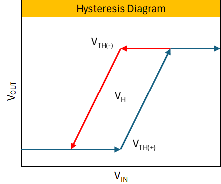
Schmitt triggers are a circuit building block frequently used to add a level of noise immunity to a circuit. They are used in many applications from hardware button de-bouncing, signal conditioning, to oscillator circuits to name a few.
Schmitt triggers work by adding hysteresis to an input signal such that it takes an additional threshold to change states. Hysteresis is added by providing feedback from the output back to the input. Once a state change is triggered the signal causing the state change must drop below the threshold point to trigger a reverse state change.
In this article a mathematical analysis of a non-inverting op-amp based Schmitt trigger is presented. Schmitt triggers are also sold in standalone integrated circuits, however, op-amps are still used to create these circuits due to their flexibility in parameter configuration.
Circuit Diagram

The circuit diagram shows a simplified non-inverting Schmitt trigger configuration using an operational amplifier. Note that while the power inputs are omitted this circuit is intended to operate with bipolar supplies. For simplicity all mathematical models assume ideal components. This could be adapted to single supply operation using an offset voltage to shift the threshold, however.
\(R_1\) and \(R_2\) form a voltage divider and positive feedback path from \(V_{out}\) to the noninverting node of the op-amp. The inverting input of the op-amp is connected to “ground” or \(0V\). This sets the offset voltage or the trigger point of the circuit.
Analysis Setup
Superposition is used to determine the voltage at the non-inverting input node. Recall that superposition is the summation of individual components in a linear system to calculate the equivalent system response.
Superposition in this example is applied by shorting voltage sources and calculating the contributions of each voltage source to the node of interest. In this case the node of interest is the non-inverting input node.
Remember that an ideal op-amp will act as a comparator when operated without negative feedback due to its high (“infinite”) gain. This means that if the non-inverting node is greater than the inverting node the output will be “high”, and if it is lower, then it will be “low”. Since the inverting node is grounded it is considered to be at \(0V\) potential. This means that the output will trigger a “high” output when the noninverting node exceeds \(0V\).
Note that “high” and “low” refer to the output saturation values which depend on supply voltage. In an ideal op-amp they will be equivalent to the rail voltages \(V_{CC}\), and \(V_{EE}\) respectively. In a real operational amplifier there will be some offsets involved.
What makes this circuit special is the voltage divider configuration which provides feedback from the output to the non-inverting node as will be analyzed by component contribution. There are two voltage sources to consider which represent the components that will be summed, \(V_{in}\) and \(V_{out}\).
$V_{in}$ Component

When observing the circuits schematic from left to right the first voltage source is \(V_{in}\). To analyze the contributions of this voltage source all other voltage sources are assumed to be short circuits. In this example there are two voltage sources, therefore \(V_{out}\) is virtually shorted in this example to calculate the contributions of \(V_{in}\).
The component from this network is simply the input voltage \(V_{in}\) multiplied by the divider ratio.
\[\Large V+ =[ V_{in} \cdot \frac{R_2}{R_1 + R_2}]\]\(V_{out}\) Component

The second component of this network is the \(V_{out}\) component. This is analyzed in the same manner as the \(V_{in}\) component except that instead of shorting \(V_{out}\) , \(V_{in}\) is shorted virtually instead.
Note that since the direction reversed the voltage divider appears in reverse. That is \(R_1\) is now the “shunt” instead of \(R_2\) hence the reversed order in the voltage divider equation.
\[\Large V+ = [ V_{out} \cdot\frac{R_1}{R_1 + R_2}]\]Resistor Reference Designators
Observe closely which resistors are used in the equation for a voltage divider. The shunt resistor to ground always goes in the top of the equation. The naming conventions can be arbitrary where reference designators do not always match the ideal naming conventions used in basic formulas.
Superposition Application - Junction Summation
The superposition principle is now applied by summing the individual voltage components to determine the system response.
\[\Large V_{+} = {V_{in}} + V_{out}\] \[\Large V_{+} = V_{in} \cdot \frac{R_2}{R_1 + R_2} + V_{out} \cdot\frac{R_1}{R_1 + R_2}\]Recall that the switching “pivot point” occurs when the voltage node is equal to zero volts. In component terms this means that components must cancel out where they are equal in magnitude but opposite in sign.
\[\Large {V_{in}} = -V_{out}\] \[\Large V_{in} \cdot \frac{R_2}{R_1 + R_2} =- V_{out} \cdot \frac{R_1}{R_1 + R_2}\]This equation can now be simplified.
\[\Large V_{in} \cdot \frac{R_2}{{\textcolor{red}{\cancel{\textcolor{black}{R_1 + R_2}}}}} =- V_{out} \cdot \frac{R_1}{\textcolor{red}{\cancel{\textcolor{black}{R_1 + R_2}}}}\] \[\Large V_{in} \cdot R_2 = -V_{out} \cdot R_1\] \[\Large V_{in} = -V_{out} \cdot \frac{R_1}{R_2}\]Offset Voltage
Note that in reality no operational amplifier behaves as an ideal component. There will always be an offset voltage that must be exceeded to trigger the output.
Switching Thresholds
The threshold voltages for a bipolar operational amplifier are derived from the pivot point.
\[\Large V_{th+} = V_{sat(+)} \cdot \frac{R_1}{R_2}\] \[\Large V_{th-} = - V_{sat(-)} \cdot \frac{R_1}{R_2}\]This equation provides the basis of the hysteresis window calculation which is the difference between the upper and lower thresholds.
\[\Large V_{H} = V_{sat(+)} \cdot \frac{R_1}{R_2} - \left( -V_{sat(-)} \cdot \frac{R_1}{R_2} \right)\] \[\Large = V_{sat(+)} \cdot \frac{R_1}{R_2} + V_{sat(-)} \cdot \frac{R_1}{R_2}\] \[\Large = \frac{2\cdot R_1}{R_2} \cdot V_{sat}\]Shifting Threshold
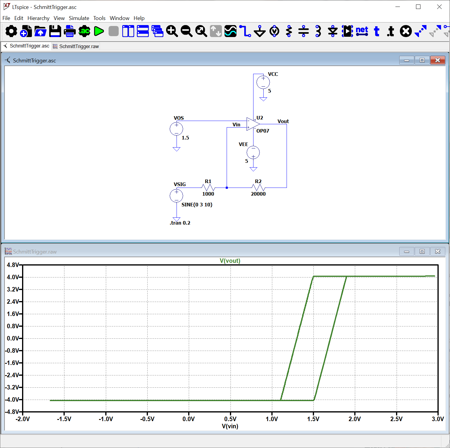
The threshold voltage can be shifted by applying an offset voltage to the inverting pin of the op-amp. This offset voltage will shift the window. This can be modeled as a sum to the threshold. Since the threshold voltage in the above equations is zero the \(V_{OS}\) term becomes zero and is therefore omitted.
\[\Large V_{TH} = V_{sat(+)} \cdot \frac{R_1}{R_2} + V_{OS}\]LTSpice Simulation
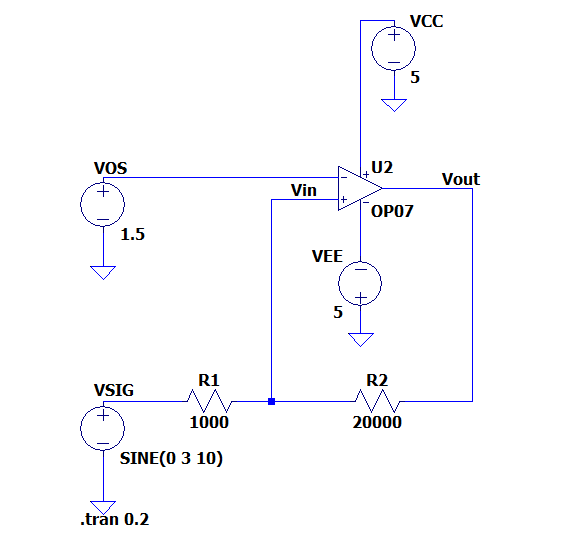
This circuit can be simulated in LTSpice by duplicating the schematic and completing the circuit with signal sources.
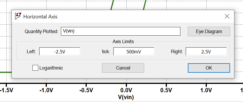
The plot can be modified such that it ouputs an X-Y style diagram instead of time on the X-axis by right clicking the horizontal axis and changing the quantity plotted as shown below.
The following plot was generated with \(V_{OUT}\) on the vertical axis, and \(V_{in}\) on the horizontal axis to result in a standard hysteresis plot.
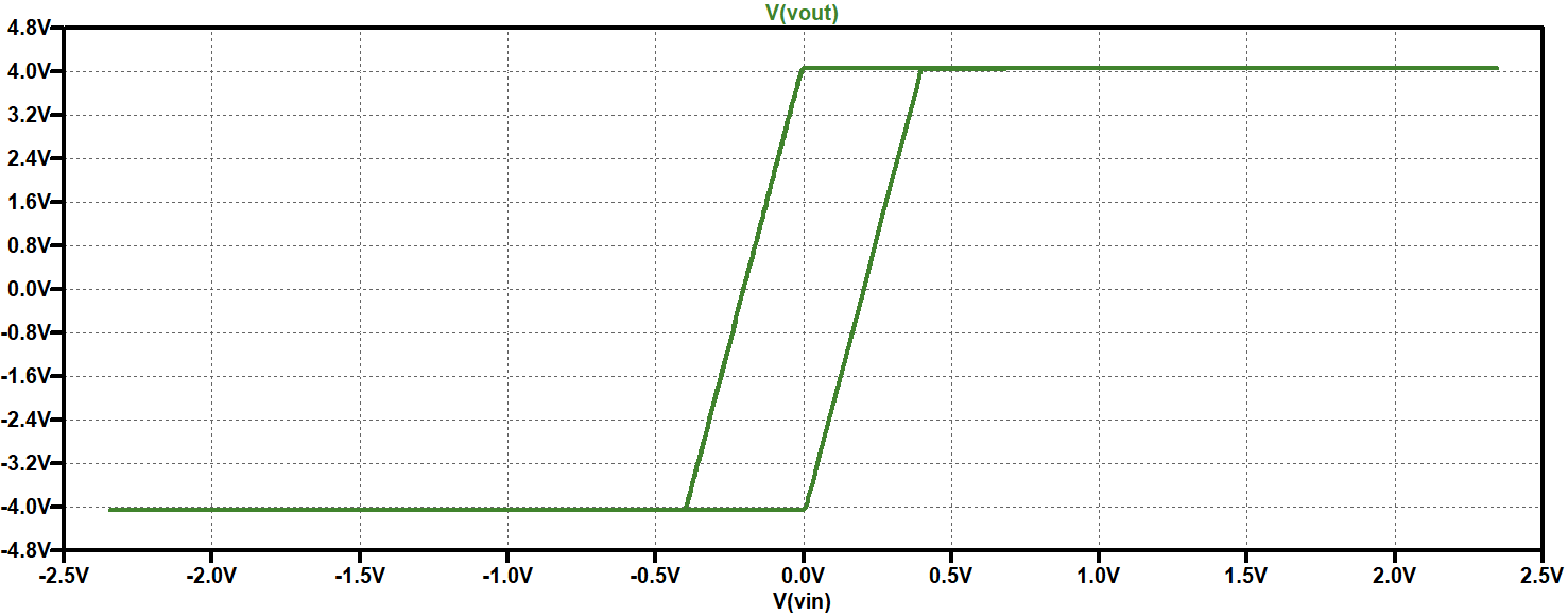
Adjusting the offset voltage shifts the threshold as expected:
Adjusting the resistance value of \(R_2\) expands the hysteresis range and can be seen as an expanded window in the plot.

Nonidealities
Implementation using real components differs from the ideal models used in the analysis. In real components op-amps have offset voltages that will shift the threshold point. They require input bias current, and have loading effects. Component parameters will change with temperature, and the resistors (and other components) have manufacturing tolerances which must be considered.
The equations are simplified, but can be expanded to encompass a tolerance stack-up. Once the limits of the components are found their worst case values can be used as calculation boundaries. This process is referred to as “extreme value analysis” and is part of “worst case analysis”. When products are manufactured in volume a statistical approach such as monte-carlo analysis could be used.
Summary
An operational amplifier makes for a multipurpose tool and when used in a Schmitt trigger configuration, enables conditioning signals to enhance operation in noisy environments. Using the superposition principle a linear system can be broken down into individual components which can be used to generate a mathematical model of a systems response.
The voltage dividers formula depend upon each resistors orientation to the system however all follow the same formula as long as the series and shunt component are considered carefully regardless of reference designator name.
The hysteresis, or window width of a Schmitt trigger depend upon the resistance values used in concert with the output voltage. The window width can be tuned by adjusting the resistance values, and the trigger level can be adjusted by application of a voltage to the noninverting pin of the op-amp.
Terms
- Saturation Voltage - The voltage presented at the output of the operational amplifier when the output is saturated, or at the maximum permissible voltage the system can get to on one of the supply rails. This voltage can be positive or negative.
- Offset voltage - The voltage difference between the two inputs of the operational amplifier required to zero the output. This can also be considered as an additional voltage required to switch the input to a different state.